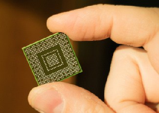
Small Electronic Circuit Design – How Small a PCB Can Be?

With advancement in technology, the consumer demand for slimmer, smaller and faster products is on the rise. As the gadgets are going smaller and smaller; they require even smaller printed circuit boards to work with.
According to market experts, this consumer demand for smaller products with more efficient functionality is not going to lower down soon. Hence, the PCB designers have to work with the growing demand and design PCBs as smaller in size as possible without compromising the functionality. However, the technology that is packed in these small electronic circuit designs to meet the ever-growing consumer demand poses major challenges to the PCB designers and fabricators as to how small a PCB they can make.
Challenges Encountered in Designing a Small PCB
- Heat Dissipation
This is the topmost of all challenges. The smaller the PCB; more tightly the components will be packed together. As a result, a smaller PCB will produce more heat. This heat requires to be dissipated; otherwise, the entire electronic circuit will get damaged ultimately damaging the electronic product as a whole.
PCB designers do have a set of methods for cooling. As well as several manufacturers are coming up with new components to help dissipate the heat. In future, however, as the PCB will grow smaller; several different layers will be stacked on one another; in an attempt to decrease the size; the heat dissipated will, undoubtedly, become more.
Hence, thermal issues are the major challenges in designing a compact printed circuit board.
- Signal Routing
As more and more complex components are crammed together in a PCB; there is a very little space left on the board for signal routing. When space is less; it is compensated by increasing the layers so as to accommodate the routing for the PCB. With more layers, as said above, heat dissipated will be more. Also, the cost of fabricating the PCBs will escalate.
- Assembly
In a smaller PCB, it is possible that the components are placed extremely close to each other and also on the board’s edge. This creates several challenges in assembly. For example; if a component is placed on the edge of the board and it slightly protrudes out; it becomes extremely difficult for the pick and place machine to work on this. Hence, precise assembly components need to be used to maintain the design of the PCB.
- Testability
A smaller PCB provides challenges to the testing part also which is done along with the assembly stage. As the components are placed extremely close to each other there is the very negligible amount of space left on the board for the placement of test points or access nodes.
Hence, several advanced testing mechanisms are used instead of the traditional testing methods. The numbers of test points required are reduced. But, with the size of PCB growing smaller and smaller in the future; it surely poses a challenge to the testability factor as well.


